


版权说明:本文档由用户提供并上传,收益归属内容提供方,若内容存在侵权,请进行举报或认领
文档简介
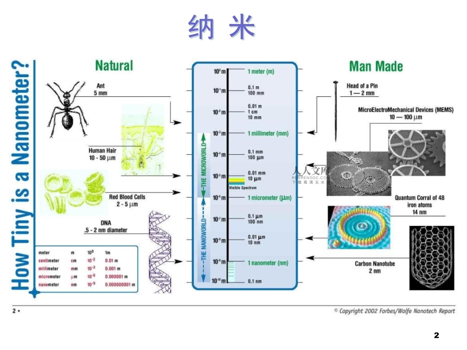
1、纳米材料与纳米科技13th May, 20091纳 米1.什么是纳米科学?2.纳米材料及其特性3.纳米技术的应用 2What is Nanometer?A nanometer is about the width of six bonded carbon atoms, and approximately 40,000 are needed to equal the width of an average human hair. DNA (width) is 2 nmProteins range from 5 to 50 nmViruses range from 75 to 100 nmA vi
2、rus is 100 nmRed blood cells are 7,000 nm in diameter, and 2000 nm in heightWhite blood cells are 10,000 nm in diameter Bacteria range from 1,000 to 10,000 nmA hydrogen atom is 0.1 nmFullerenes (C60 / Buckyballs) are 1 nm Quantum Dots (of CdSe) are 8 -50 nm Dendrimers are 10 nmNanoparticles range fr
3、om 1 to 100 nm3Importance“One nanometer is a magical point on the dimensional scale. Nanostructures are at the confluence of the smallest of the human-made devices and the largest molecules of living things. Nanoscale science and engineering here refer to the fundamental understanding and resulting
4、technological advances arising from the exploitation of new physical, chemical and biological properties of systems that are intermediate in size, between isolated atoms and molecules and bulk materials, where the transitional properties between the two limits can be controlled.”M.C. Roco (National
5、Science Foundation), 2001.4Theres Plenty of Room at the Bottomby Richard P. Feynman December 29th 1959 年,诺贝尔奖获得者、理论物理学家理查得费因曼教授在加州理工大学发表了题为在底部还有很大空间的演讲。在费因曼看来,人类社会目前的生产方式,总是“从上而下(top-down Manufacturing)”的,他提出:为什么我们不可以从单个分子、甚至原子开始出发进行组装 (bottom-up manufacturing) ,达到我们的要求?物理学的规律不排除一个原子一个原子制造物品的可能。”(纳米
6、科学的开山之作) 5Nanoscience Study of fundamental principles of molecules and structures with at least one dimension roughly between 1 and 100 nm. Nanotechnology- sometimes shortened to nanotech, refers to a field of applied science whose theme is the control of matter on an atomic and molecular scale. Gen
7、erally nanotechnology deals with structures 100 nanometers or smaller, and involves developing materials or devices within that size.Nanostructures Smallest solid things it is possible to make.67“Nanotechnology is likely to be particularly important in the developing world, because it involves littl
8、e labour, land or maintenance; it is highly productive and inexpensive; and it requires only modest amounts of materials and energy” UN Millennium Project. “Nanoscience and technology will change the nature of almost every human-made object in the 21st century” - M.C. Roco, R.S. Williams, P. Alivisa
9、tos, 1999 the National Science and Technology Council “Just waitthe 21st century is going to be incredible. We are about to be able to build things that work on the smallest possible length scales, atom by atom. These nanothings will revolutionize industries and our lives” - Richard Smalley, 1999 (1
10、996 noble prize in chemistry)The convergence of nanotechnology with information technology, biology and social sciences will reinvigorate discoveries and innovation in many areas of the economy. - George W. Bush, President of the United States7Macroscale vs. Nanoscale Gold 8Nano-sizing Causes Change
11、s In Melting point:Macroscale vs. Nanoscale Gold Nanoscale Materials in Chemistry, K. J. Klabunde, ed., Wiley, 2001, Chapter 8.9一、C60近年来,科学家们发现,除金刚石、石墨外,还有一些新的以单质形式存在的碳。其中发现较早并已在研究中取得重要进展的是C60分子。C60分子是一种由60个碳原子构成的分子,它形似足球,因此又名足球烯。10Nanoscience is a subject defined by its dimension. Sometimes its fun
12、 to play with that a little. If a buckyball was as big as a football, a football would be as big as the earth! These flourinated fullerenes come from the work of Roger Taylor and Adam Darwich 1112制作过程足球烯是美国休斯顿赖斯大学的克罗脱和史沫莱等人于1985年提出的。他们用大功率激光束轰击石墨使其气化,用1MPa压强的氦气产生超声波,使被激光束气化的碳原子通过一个小喷嘴进入真空膨胀,并迅速冷却形成新
13、的碳原子,从而得到了C60。13Fullerene Science1985: C60-discovered (Nature 318, 162) 1990: C60-macroscopic scale synthesis (Nature 347, 354)1991: Carbon nanotubes-discovered (Nature 354, 56)1996: Noble prize for C601415C60的应用气体的贮存在控制温度和压力的条件下,可以简单地用C60和氢气制成C60的氢化物,它在常温下非常稳定,而在80 215 时,C60的氢化物便释放出氢气,留下纯的C60,它可以被1
14、00%地回收,并被用来重新制备C60的氢化物。与金属或其合金的贮氢材料相比,用C60贮存氢气具有价格较低的优点,而且C60比金属及其合金要轻。C60的应用16因此,相同质量的材料,C60所贮存的氢气比金属或其合金要多。C60不但可以贮存氢气,还可以用来贮存氧气。与高压钢瓶贮氧相比,高压钢瓶的压力为3.9106 Pa,属于高压贮氧法,而C60贮氧的压力只有2.3105 Pa,属于低压贮氧法。利用C60在低压下大量贮存氧气对于医疗部门、军事部门乃至商业部门都会有很多用途。17有感觉功能的传感器由于用C60薄膜做基质材料可以制成手指状组合型的电容器,用它来制成的化学传感器具有比传统的传感器尺寸小、简
15、单、可再生和价格低等优点,可能成为传感器中颇具吸引力的一种候选产品。18此外提高金属硬度应用于新型催化剂对光的限制性可应用于对人的眼睛的保护对癌细胞杀伤抑制人体免疫缺损蛋白酶的活性充当水溶性抗氧剂 等等19纳米材料纳米材料: 在纳米量级(1100nm)内调控物质结构制成的具有特异性能的新材料四大特点: 尺寸小、比表面积大、表面能高、表面原子比例大四大效应: 小尺寸效应、量子尺寸效应、宏观量子隧道效应、表面效应纳米材料特性取决于制备方法20纳米材料应用21环境:处理汽车尾气含铅汽油中的铅很容易通过血液长期蓄积于人的肝、肾、脾、肺和大脑中,从而导致人的智能发育障碍和血色素制造障碍等后果。汽车尾气的
16、处理:加入纳米级的复合稀土氧化物后,对尾气的净化特别明显,尾气中的CO、NOx几乎完全转化。22水处理特种半导体纳米材料使海水淡化;纳米TiO2可以用来降解有机磷,降解毛纺染整废水,降解石油 23能源:储氢碳纳米管是直径非常细的中空管状纳米材料,它能够大量地吸附氢气,成为许多个“纳米钢瓶” 。研究表明,约2/3的氢气能够在常温常压下从碳纳米管中释放出来。据预测,到2010年,就可以生产出氢气汽车,只需携带1.5升左右的储氢纳米碳管,即可行驶500km。24纳米碳管25防弹衣因纳米碳管既轻又强度极高,是钢的10100倍,用它来作防弹衣就像用羽绒做成的防寒服一样,既可折来叠去,又能抵御强大的子弹的
17、冲击力。26纳米泵人造红细胞它比体内血液中的红细胞要多携带200多倍的氧气。血液形态图 27靶向给药美国麻省理工学院的研究人员研究一种只有20nm的药物炸弹和包含了1000个纳米药包的微型芯片;在固定的DNA链上连接上杀癌的药物胶囊,放到病人血液和组织内,一遇上癌细胞的DNA时,DNA链就与癌细胞的DNA结合,这时药物开关受触发而开放,药物便释放出来,杀灭癌细胞;28 生物医药:纳米清洁工科学家设想制造出负责清扫血管的纳米机器人(清洁工),专门负责清扫血管壁上的胆固醇、凝血等沉积物,以预防脑血栓等心血管病;同时也可以制作出清扫体内癌细胞的机器人。29太空云梯坚韧的碳纤维,其密度是钢的1/6,强
18、度为钢的10100倍,重量则只有钢的1/4。将纳米碳管做成太空升降机的缆绳,由于它的强度高、重量轻,即使是从太空下垂到地面,它也完全可以承受自身的重量而不会断开,它是目前唯一可作为太空云梯的理想材料。30日常生活纳米TiO2:在光照条件下,会产生具有非常强的氧化能力的空穴,从而将附在表面上的有机物、细菌及其它灰尘分解掉,直至生成CO2和H2O。杀菌、除味:由于纳米ZnO具有大的比表面积,可以很快地吸收并分解臭气,同时还能有效地杀菌。对黄色葡萄球菌和大肠杆菌的杀菌率高达95%以上。抗菌纳米服装:不用清洗信不信由你31军事吸波:纳米ZnO对雷达电磁波具有很强的吸收能力,所以可以做隐形飞机的重要涂料
19、。322005年10月20日报道, 目前美国Nice大学的科学家研制出世界第一辆单分子纳米汽车。该汽车在显微镜下可见的金属道路上行驶。车轮是球型的,由包含60个原子的单质碳构成。整辆汽车对角线的长度仅为34纳米,比单股的DNA稍宽。相比而言,人一根头发的直径大约是80,000纳米。纳米汽车33纳米管收音机2007 年,美国加利福尼亚大学伯克利分校的物理学家亚历克斯策特尔(Alex Zettl) 。在该碳纳米管收音机中,碳纳米管承担了收音机的天线、调谐器、放大器和解调器等诸多部件的功能。如图1所示,纳米收音机的碳纳米管被置于真空管中,并将一端固定在电池的负极上。碳纳米管的另一端(即自由端)和电池
20、正极之间留有纳米量级的间隙。如果电极间的电压足够高,正极能将碳纳米管自由端的电子夺过来。当广播电台的无线电信号经过该碳纳米管收音机时,其产生的电场将不断“推”和“拉”纳米管的自由端,也就是碳纳米管随无线电信号发生共振,利用这种共振现象及回路中相应的电流变化就可以探测到无线电信号。这里,回路中受无线电信号感应得到的高频交变电流信号后经碳纳米管“调谐”、“放大”和“解调”后,便会转化为携带声音信息的低频信号,进而,通过喇叭等播出声音。 34万能关节Name: Universal JointDesigner: Mark Sims, based on a 1992 design by K. Eric
21、Drexler and Ralph MerkleDate: May 25, 2006Number of components: 4 (which form a single covalent structure)Number of atoms: 3,846Width: 3.8 nmHeight: 3.8 nmLength: 6.4 nm (not including shafts) 35世界最小的纳米电动机:以碳纳米管为轴,金片为叶,在电流驱动下转动 36ATP分子马达 该生物马达由腺苷三磷酸酶ATP吸附在镍螺旋桨周围,并给主轴提供能量37利用碳纳米管制造出一种奇妙的纳米秤,这种秤竟然可以称出
22、单个原子的重量。之所以选用碳纳米管来作为制作纳米秤的材料,是因为碳纳米管中间是空的,而且质量非常轻,对原子的振动非常敏感,这样可以更准确的“秤”出原子的重量 。不过它并不是利用杠杆原理来称量原子的重量。这种纳米秤实际上是一个悬臂,类似于跳水运动员使用的跳板,长约250纳米,一头固定在一个电极上,另一头则不固定。当一个原子落下掉在这个悬臂上,原子的重量会引起悬臂进行振动。这就像跳水板一样,跳水运动员的体重不同,跳水板的振动频率和幅度也会有相应的变化。然后他们利用振动频率的差异来测算出原子的重量。 纳米秤3839nano guitar playable and coloredA nanoguita
23、r, devised at Cornell years ago, has been played for the first time by shooting laser light at the silicon strings. A newer version of the guitar, shown above, twangs at a frequency of 40 megahertz, some 17 octaves (or a factor of 130,000) higher than a normal guitar. Electron-microscope image of th
24、e worlds smallest guitar. Its length is 10 micrometers (10 millionths of a meter).Thats about the size of a red blood cell and about 1/20th the width of a single human hair. Its strings have a width of about 50 nanometers (the size of approximately 100 atoms). If you were to pluck the tiny strings t
25、hey would produce a high-pitched sound at the inaudible frequency of approximately 10 megahertz. Made by Cornell researchers with a single silicon crystal using the techniques of high voltage electron beam lithography, this tiny guitar is a fun example of nanotechnology.Many of the same techniques a
26、re applied by scientists building machines and devices on the nanometer scaleto perform useful technological functions and study submicroscopic processes. 40纳米上的艺术41纳米尺度的世界名画! (a)原画(b)纳米摹本 新加坡国立大学科学家利用离子束写入技术,把十九世纪英国画家威廉布莱克的经典名画转移到了可以精细调节的纳米晶体上。科学家称之为“量子艺术”。精度为100微米,细节尺寸达到纳米量级。42诱人的纳米棒棒糖这是一张电子显微镜照片,
27、显示的是一个微观的纳米结构,该结构酷似一个诱人的棒棒糖。 在两个镍电极间的一根硅纳米线。右边,纳米线连着一个小的纳米镍金属球,看起来就象是个棒棒糖。所以叫它纳米棒棒糖。此图由日立S-4700场发射扫描电镜拍摄。43美国NASA用分子动力学模拟的分子齿轮(视频) (a)分子齿轮 (b)分子齿轮温度及角速度随时间的变化44搭建在一根头发上的体育场馆 采用离子束加工技术,日本学者Shinji MATSUI在一根头发上成功搭建了体育场。45 日本学者2006年利用FIB-CVD 技术制备的纳米LRC电子电路。46nanocupProfessor Shinji Matsuis research grou
28、p at the Himeji Institute of Technology (HIT) and Seiko Instruments Inc. (SII), have made the worlds smallest wine glass. Using highly advanced manufacturing techniques that can produce three dimensional (3D) objects at the nanometer scale, researchers built the glass from carbon with an external di
29、ameter of only 2,750 nanometers (nm), approximately 200,000 times smaller than a normal sized glass. 47nanocup48Nano flowers49NASA科研人员制备的Si纳米结构 50纳米向日葵(美国康纳尔大学科技人员制备的葸氢醌二乙酸酯纳米结构) 51522006, made from zinc oxide by Yujin Chen and colleagues at Harbin Engineering University,For alcohol detection53超疏水 S
30、nO2 nanoflowers54a)硫化镉纳米花 (CVD方法)美国能源部:Sandia国家实验室55Carbon上生长的锑纳米草 (新西兰科学家的AFM照片)56Si上生长的硫化钼纳米锥 (新加坡国立大学电镜照片) 57北京大学纳米中心的学者通过AFM针尖对基质Au-Pa合金上的机械刻蚀,书写了世界上最小的唐诗(10微米10微米)5859DNA 美洲地图60Nanoman was created by focussed electron beam deposition on the tip of an STM - an illustration of 3D nanostructure fa
31、brication with a precision of 10nm. 61“小人嘴脸” 这时美国加利福尼亚技术学院的科学家绘制的世界上最小的“小人”笑脸。使用的材质为DNA分子链,笑脸的尺寸为仅为几百纳米。62原子小人这是科学家通过原子力显微镜操纵28 个碳原子在铂表面上拼成的小人,28个原子组成的“人”.63Nano toilet在实验室里化学家一不小心在Si表面生成了上述“坐便器”形状的纳米结构,这应该是世界上最小的“坐便器”了,您需要电子显微镜才能看得到。64Micro-bull fabricated by FIB65分子的艺术 蚂蚱酮 它是从一种不能飞的蝗虫Romalea micro
32、ptera用于防御的分泌物中提取的.科学家们在田野里辛苦地逮蚂蚱、并惹恼它们,再从它们身上“挤奶”得到这种物质,专注的科学家太累了而不想辛苦的对它系统命名,所以他们使用了这个有创意的名字蚂蚱酮。 66纳米莆田分子 这涉及到如何合成拟人的分子(anthropomorphic molecules),即分子结构看起来就像是一个人。它们(指分子)有着不同的形式,但基本的形式被称为“纳米孩子”(NanoKid),从这里出发,其他不同形式的分子可以被合成,例如“纳米运动员”(NanoAthlete)和“纳米面包师”(NanoBaker)。 国王运动员面包师学者厨师特种部队队员小丑德克萨斯人朝圣者67企鹅酮
33、由于它分子的二维结构式类似一只企鹅,所以被命名为“企鹅酮”(Penguinone),但是这种效果在三维模型中却失去了。它的系统命名应该是 3,4,4,5-tetramethylcyclohexa-2,5-dienone. 6869纳米材料的常见制备方法70The scanning electron microscopic image of a 3D macroporous material that was fabricated by infiltrating a 3D opaline lattice of silica spheres with a hexane solution conta
34、ining buckyballs. Note that the porous features underneath were also visible through the pores on the surface of the membrane.Typical fabrication模板合成71纳米芯壳结构The scanning electron microscopic image of a 3D crystalline lattice assembled from AuSiO2 core-shell colloids. The gold cores were 50 nm in dia
35、meter and the silica shells were 120 nm in thickness. 72氧化铝模板DpDc73Fabricated in 0.3 M oxalic acid solution, 40V, 2 oCTypical SEM images of as-prepared AAO templates74SEM images of Co nanowires fabricated by pulse DC electrodeposition(a)(b)(c)(d)75以粒径为6微米的金红石相氧化钛为原料,制备无定形氧化钛纳米粉体的过程:TiO2粗粉水洗20M,NaOH,
36、200oC无定形氧化钛300oC热处理0.5h水热法76无定形氧化钛0.2M HCl1.0M HCl水洗水洗锐钛矿相金红石相(a): 无定形氧化钛产物, (b): 锐钛矿相氧化钛产物, (c): 金红石相氧化钛产物.7720M,NaOH130oC-170oCTiO2微米粉体水洗纳米管20M,NaOH200oC-250oC水洗纳米丝78Schematic illustration of vapor-liquid-solid nanowire growth mechanism including three stages (I) alloying, (II) nucleation, and (II
37、I) axial growth.CVD制备纳米线79(a) SEM image of ZnO nanowires synthesized via the VLS mechanism (b) TEM images of the single-crystalline ZnO nanowires.80SEM (a, c) and cross sectional TEM (b) images of SnO2 nanobelts obtained by evaporation and condensation of SnO at 1000 oC.81ZnO nanowire arrays on sapp
38、hire substrate. Huang M., Mao S., Feick H., Yan H., Wu Y., Kind H., Weber E., Russo R., and Yang P., Room-temperature ultraviolet nanowire nanolasers, Science 292(2001) pp.1897-189982Site-selective growth of ZnO nanowire arrays on a-plane sapphire substrates. The pattern of nanowire array is defined
39、 by the initial Au thin film pattern fabricated by photolithography.Science 292(2001) pp.1897-189983STEM image of two nanowires in bright field mode. The scale bar is 500 nm. (b) Line pro EDS signal from Si and Ge components along the nanowire growth axis. Wu Y., Fan R. and Yang P., Block-by-Block G
40、rowth of Single-Crystalline Si/SiGe Superlattice Nanowires, Nano Lett. 2(2002) pp.83-86.84Electrical field induced nanowire alignment represents another powerful assembly technique. Lieber et al. have fabricated metal electrode arrays on which bias is applied to generate strong electrical filed to a
41、lign Si and InP nanowires dispersed in between the electrodes(b). Typical SEM images of crossed arrays of InP nanowires obtained in a two-step assembly process with orthogonal flow directions for the sequential steps. Flow directions are highlighted by arrows in the images. The scale bar corresponds
42、 to 2 m.The microchannels are formed between a flat Si/glass substrate. A droplet of the wire solution/suspension was placed at the open end of the microchannels; the liquid fills the channels under capillary effect. After the evaporation of the solvent, wires were aligned along the edges of the microchannels。(a)SEM image of the aligned Mo3Se3 - molecular wire bundles on Si wafer. Inset shows the cross-junction formed through multiple layer alignment process. 纳米线的排列85The melting starts from two ends at around 650 o
温馨提示
- 1. 本站所有资源如无特殊说明,都需要本地电脑安装OFFICE2007和PDF阅读器。图纸软件为CAD,CAXA,PROE,UG,SolidWorks等.压缩文件请下载最新的WinRAR软件解压。
- 2. 本站的文档不包含任何第三方提供的附件图纸等,如果需要附件,请联系上传者。文件的所有权益归上传用户所有。
- 3. 本站RAR压缩包中若带图纸,网页内容里面会有图纸预览,若没有图纸预览就没有图纸。
- 4. 未经权益所有人同意不得将文件中的内容挪作商业或盈利用途。
- 5. 人人文库网仅提供信息存储空间,仅对用户上传内容的表现方式做保护处理,对用户上传分享的文档内容本身不做任何修改或编辑,并不能对任何下载内容负责。
- 6. 下载文件中如有侵权或不适当内容,请与我们联系,我们立即纠正。
- 7. 本站不保证下载资源的准确性、安全性和完整性, 同时也不承担用户因使用这些下载资源对自己和他人造成任何形式的伤害或损失。
最新文档
- 各办公室卫生管理制度
- ktv卫生组织制度
- 单生产车间卫生制度
- 公共卫生间客户专用管理制度
- 美发美容店卫生安全制度
- 村卫生室疫情救治设备管理制度
- 村委会卫生大扫除制度
- 防静电车间卫生打扫制度
- 食品工器具清洁卫生制度
- 母婴店上班卫生规章制度
- 中药学教材课件
- 梦虽遥追则能达愿虽艰持则可圆模板
- 能源与动力工程测试技术 课件 第一章 绪论确定
- 配件售后管理制度规范
- 浙江省绍兴市上虞区2024-2025学年七年级上学期期末语文试题(解析版)
- 《隶书千字文》-清席夔
- 2024校长在寒假期末教职工大会上精彩发言主要引用3个关键词善待自己改变自己提升自己
- 《铁路技术管理规程》(普速铁路部分)
- 2024-2025年度“地球小博士”全国地理科普知识大赛参考试题库(含答案)
- 北师大版六年级上册分数混合运算100题带答案
- 2024年度工程成本控制优化合同
评论
0/150
提交评论