


版权说明:本文档由用户提供并上传,收益归属内容提供方,若内容存在侵权,请进行举报或认领
文档简介
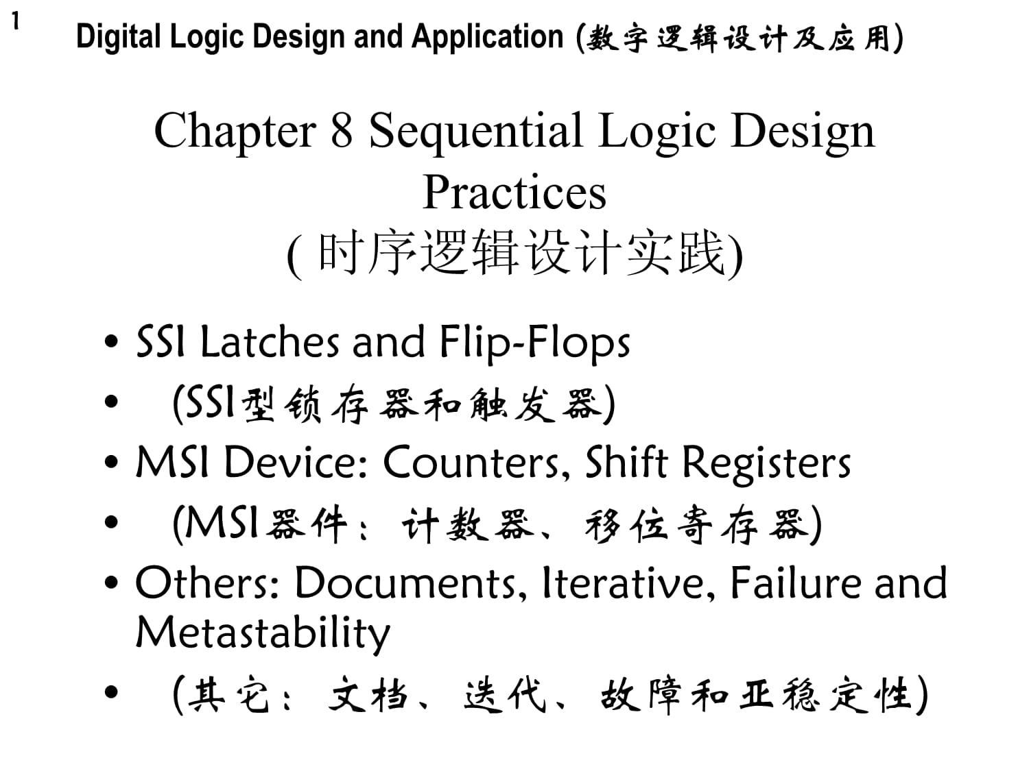
1、Chapter 8 Sequential Logic Design Practices ( 时序逻辑设计实践)SSI Latches and Flip-Flops (SSI型锁存器和触发器)MSI Device: Counters, Shift Registers (MSI器件:计数器、移位寄存器)Others: Documents, Iterative, Failure and Metastability (其它:文档、迭代、故障和亚稳定性)Digital Logic Design and Application (数字逻辑设计及应用)1Chapter 8 Sequential Logic
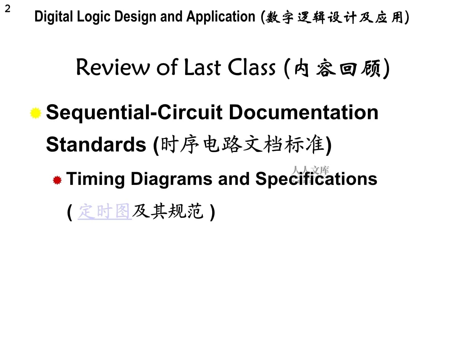
2、DesReview of Last Class (内容回顾)Sequential-Circuit Documentation Standards (时序电路文档标准)Timing Diagrams and Specifications ( 定时图及其规范 )Digital Logic Design and Application (数字逻辑设计及应用)2Review of Last Class (内容回顾)SeqReview of Last Class (内容回顾)Latches and Flip-Flops (锁存器和触发器)SSI Latches and Flip-Flops (SSI型锁
3、存器和触发器)Applications: Switch Debouncing, Bus Holder (应用:开关消抖、总线保持)Multibit Registers and Latches( 多位寄存器和锁存器 )Digital Logic Design and Application (数字逻辑设计及应用)3Review of Last Class (内容回顾)Lat8.4 Counter (计数器)Modulus: The number of states in the cycle (模:循环中的状态个数)A modulo-m counter, or sometimes, a divid
4、e-by-m counter ( 模m计数器, 又称 m分频计数器)Any clock sequential circuit whose state diagramContain a Single cycle.(状态图中包含有一个循环的任何时钟时序电路)Digital Logic Design and Application (数字逻辑设计及应用)48.4 Counter (计数器)Modulus: The8.4 Counter (计数器)An n-bit binary counter (n位二进制计数器)S1S2S3SmS5S4ENENENENENENENENENENENENENDigita
5、l Logic Design and Application (数字逻辑设计及应用)58.4 Counter (计数器)An n-bit binA Synchronous Binary Up Counter(同步二进制加法计数器)1 0 1 1 0 1 1+ 11 0 1 1 1 0 0在多位二进制数的末位加 1,仅当第 i 位以下的各位都为 1 时,第 i 位的状态才会改变。最低位的状态每次加1都要改变。Qi* = (Qi-1 Q1 Q0) QiQ0* = 1 Q0Digital Logic Design and Application (数字逻辑设计及应用)6A Synchronous B
6、inary Up CounteA Synchronous Binary Up-Counter(同步二进制加法计数器) 利用有使能端的 T 触发器实现:Q* = EN QENi = Qi-1 Qi-2 Q1 Q0 利用 D 触发器实现:Di = (Qi-1 Q1 Q0) QiQi* = (Qi-1 Q1 Q0) QiQ0* = 1 Q0Digital Logic Design and Application (数字逻辑设计及应用)7A Synchronous Binary Up-CounteMSI Counters (MSI计数器)74x161、74x1634-Bit Binary Up-Cou
7、nters (with Asynchronous/Synchronous Clear) (4位二进制加法计数器(异、同步清零))74x160、74x1621-Bit Decade (BCD Code) Up-Counters (with Asynchronous/Synchronous Clear)(1位十进制(BCD)加法计数器(异、同步清零))Digital Logic Design and Application (数字逻辑设计及应用)8MSI Counters (MSI计数器)74x161、74MSI Counter (MSI计数器)74x1694-Bit Binary Up/Down
8、 Counter(4位二进制可逆计数器)计数器可以用作分频器Digital Logic Design and Application (数字逻辑设计及应用)9MSI Counter (MSI计数器)74x169DigiAny Modulus Counter(任意模值计数器)利用SSI器件构成 时钟同步状态机设计利用MSI计数芯片构成 利用n位二进制计数器实现模m计数器分两种情况考虑: m 2n 清零法、置数法Digital Logic Design and Application (数字逻辑设计及应用)10Any Modulus Counter(任意模值计数器)利Any Modulus Cou
9、nter(任意模值计数器)Realize a Modulo-m Counter with an n-bit Binary Counter (利用n位二进制计数器实现模m计数器)Digital Logic Design and Application (数字逻辑设计及应用)11Any Modulus Counter(任意模值计数器)DAny Modulus Counter(任意模值计数器)Consider two cases(分两种情况考虑): m 2nS0S1S2S3S4S12S11S10S9S8S7S6S5S13S14S15清零法、置数法级联。Digital Logic Design and
10、 Application (数字逻辑设计及应用)12Any Modulus Counter(任意模值计数器)CCascading Counter (计数器的级联)CLOCKRESET_LLOAD_LCNTEND0D1D2D3Q4Q5Q6Q774x16374x163思考:利用低位的进位控制高位的时钟行不行?Digital Logic Design and Application (数字逻辑设计及应用)13Cascading Counter (计数器的级联)CLOCModulo-m Counter(模m计数器( m 2n))先进行级联,再整体置零或预置数例:用74x163构造模193计数器 两片1
11、63级联得8位二进制计数器(0255) 采用整体清零法,0192 采用整体预置数法,63255 25619363若 m 可以分解:m = m1m2分别实现m1和m2,再级联Digital Logic Design and Application (数字逻辑设计及应用)14Modulo-m Counter(模m计数器( m 26310 = ( 0011 1111 )2 CLKCLRLDENPENTA QAB QBC QCD QD RCO74x163 CLKCLRLDENPENTA QAB QBC QCD QD RCO74x16311001111+5VCLOCKCLR_LDigital Logic
12、 Design and Application (数字逻辑设计及应用)156310 = ( 0011 1111 )2 CLK74x1 CLKCLRLDENPENTA QAB QBC QCD QD RCO74x163 CLKCLRLDENPENTA QAB QBC QCD QD RCO74x16311001111CLOCKCLR_L+5VQ4Q5Q6Q7ENDigital Logic Design and Application (数字逻辑设计及应用)16 CLK74x163 CLK74x16311CLOCKCAnalysis what the modulo of the following c
13、ircuit is ?(分析下面的电路的模为多少?) CLKCLRLDENPENTA QAB QBC QCD QD RCO74x163011+5VCLOCKQD QC QB QA0 0 0 00 1 1 00 1 1 11 0 0 01 1 1 01 1 1 1Digital Logic Design and Application (数字逻辑设计及应用)17Analysis what the modulo of thExercise: Analysis what the modulo of the following circuit is ? (练习:分析下面的电路的模为多少?) ? CLK
14、CLRLDENPENTA QAB QBC QCD QD RCO74x16301+5VCLOCK模12计数器QD:12分频占空比50Digital Logic Design and Application (数字逻辑设计及应用)18Exercise: Analysis what the mo8.5 Shift Register(移位寄存器)Serial Input(串行输入)SERINSEROUTSerial Output(串行输出)Serial-In,Serial-Out(串入串出移位寄存器)Can be used to delay aSignal by n clock ticks(可以使一个
15、信号延迟n 个时钟周期之后再输出)Digital Logic Design and Application (数字逻辑设计及应用)198.5 Shift Register(移位寄存器)SeriSerial-In, Parallel-Out Shift Register(串入并出移位寄存器)Serial-In(串入)SERIN1Q2QNQParallel-Out(并出)Can be used to perform Serial-to-Parallel Conversion(可以用来完成串并转换)Digital Logic Design and Application (数字逻辑设计及应用)20S
16、erial-In, Parallel-Out ShiftParallel-In, Serial-Out (并入串出移位寄存器)多路复用结构LOAD/SHIFTSERINSEROUTDigital Logic Design and Application (数字逻辑设计及应用)21Parallel-In, Serial-Out (并入串出移Parallel-In, Parallel-Out (并入并出移位寄存器)LOAD/SHIFTSERIN1Q2QNQDigital Logic Design and Application (数字逻辑设计及应用)22Parallel-In, Parallel-
17、Out (并入并8.5.2 MSI Shift Register (MSI移位寄存器) CLKCLRSERASERB74x164QAQBQCQDQEQFQGQH CLK CLKINHSH/LDCLRSERABCDEFGH QH74x166SERASERBDigital Logic Design and Application (数字逻辑设计及应用)238.5.2 MSI Shift Register (M4-Bit Universal Shift Register (4位通用移位寄存器74x194) CLKCLRS1S0LIND QDC QCB QBA QARIN74x194S1 S0 功能0
18、 0 保持0 1 右移1 0 左移1 1 载入Left Shift Input:From QD to QA (左移输入)Right Shift Input:From QA to QD(右移输入)Digital Logic Design and Application (数字逻辑设计及应用)244-Bit Universal Shift Registe00S1S0保持S1 S0S1 S010左移01右移11载入Figure 8-41Qi* = S1S0Qi + S1S0Qi-1 + S1S0Qi+1 + S1S0INiDigital Logic Design and Application (数
19、字逻辑设计及应用)4-Bit Universal Shift Register (4位通用移位寄存器74x194)2500S1S0保持S1 S0S1 S010左移0S1 S0 功能0 0 保持0 1 右移1 0 左移1 1 载入LIN QHHQHCLR GQG CLK FQFS1 EQES0 DQDG1 CQCG2 BQBAQARIN QA74x299Use Bidirectional Three-State lines for Input and output(输入输出采用双向三态数据线)Digital Logic Design and Application (数字逻辑设计及应用) 8-B
20、it Universal Shift Register (8位通用移位寄存器)26S1 S0 功能0 0 保持LIN CLKCLRS1S0LIND QDC QCB QBA QARIN74x194 CLKCLRS1S0LIND QDC QCB QBA QARINCLKCLRS1S0LINRIN移位寄存器的扩展ParallelInputs(并行输入(8位))ParallelOutput(并行输出8位)27 CLK74x194 CLKCLKLINRIN移Para8.5.3 Shift-Register Counters(移位寄存器计数器)D0 = F ( Q0 , Q1 , , Qn-1 )Feedback Logic (反 馈 逻 辑)D Q CK QD Q CK QD Q CK QD Q CK QCLKFF0FF1FF2FF3General Structure (一般结构):Digital Logic Design and Application (数字逻辑设计及应用)288.5.3 Shift-Register Counters1000010000010010有效状态其他状态8.5.4
温馨提示
- 1. 本站所有资源如无特殊说明,都需要本地电脑安装OFFICE2007和PDF阅读器。图纸软件为CAD,CAXA,PROE,UG,SolidWorks等.压缩文件请下载最新的WinRAR软件解压。
- 2. 本站的文档不包含任何第三方提供的附件图纸等,如果需要附件,请联系上传者。文件的所有权益归上传用户所有。
- 3. 本站RAR压缩包中若带图纸,网页内容里面会有图纸预览,若没有图纸预览就没有图纸。
- 4. 未经权益所有人同意不得将文件中的内容挪作商业或盈利用途。
- 5. 人人文库网仅提供信息存储空间,仅对用户上传内容的表现方式做保护处理,对用户上传分享的文档内容本身不做任何修改或编辑,并不能对任何下载内容负责。
- 6. 下载文件中如有侵权或不适当内容,请与我们联系,我们立即纠正。
- 7. 本站不保证下载资源的准确性、安全性和完整性, 同时也不承担用户因使用这些下载资源对自己和他人造成任何形式的伤害或损失。
评论
0/150
提交评论